Sunday, June 15, 2014

Reverse engineering of serial communications

Unfortunately I end up quite often with some kind of device that has an RS-232 or RS-485 port, but that I don't have any idea what baud rate it uses, comms protocol, etc. 

I will not say that it is easy but, if you're lucky, you can get it. The direct way (and also the hard one) would be using a serial converter such as the MOXA UPort 1250 and a comm analyzer software such as Docklight (much better than the old but useful Hyperterminal). Just in case you fail using the usual standard configurations such as 9600/8/n/1 and so on, you could also be trying for some hours the other hundred of combinations for baud rate, parity bit, stop bits, etc...but as sometimes you're not lucky, I will explain here how you could reverse serial communications:

1. The first thing is to discover whether it uses RS-232 or RS-485 communications. It seems obvious, but sometimes you can not trust what they tell you. Be sure!. 

2. You should also know the Tx pin (in case of RS-232 comm) or Line A/B pins if it is a RS-485 communication. Simply hook up an oscilloscope and set the scope to trigger on a pulse. 


Fig.1: Select a pulse trigger and try to catch a complete frame


3. Once you can see a frame with your oscilloscope, you must measure the time of the shortest pulse and take the reciprocal to figure out the baud rate. 
So change the trigger mode from the usual Auto to Single and try to get a single shot of the frame. 


Fig. 2: Select Trigger Single mode and capture a single shot of the frame


4. Now select a smaller time/div to zoom in into the frame bits.


Fig 3: Move the Horizontal position knob to watch the end of the frame. You should see the final stop bit


Fig 4: Continue zoom in until you can see clearly the bits width


Fig 5: Get the best time/div that allows you measuring the bit width


5. You can now use the oscilloscope vertical cursors to measure the time between the falling and the rising edge of a bit. Of course you are not going to get an exact number of baud rate, but you will realize easily about the closest value. 


Fig. 6: Single bit width is 52 us aprox. so baud rate is 1/52us = 19200 baud 


TimeBaud Rate
3333µs300
833µs1200
416µs2400
208µs4800
104µs9600
69µs14400
52µs19200
34µs28800
26µs38400
17.3µs57600
8µs115200
4.34µs230400


6. So far this was the easy thing. Now comes the hard one: discover how many data bits are in the frame, whether it uses parity or not, if it uses one stop bit, flow control, bla bla bla...

I usually try to enumerate the latest bytes, as shown in the figure below. 


Fig. 7: Try to enumerate as many bits as you can

7. Try to identify the start and the stop bits. Let's consider most of the communications use 8 data bits and at least one stop bit, so starting from the ending stop bit backwards, you could try to identify where the start bit could be

Once you had identified both start and stop bits, it is easy to discover if it uses any parity bit. In this example if uses 1 start bit, 8 data bits, 1 even parity bit and 1 stop bit.


Fig. 8: Try to identify several transmission bytes

8. Bear in mind that in most common serial communications LSB (Least Significant Bit) is typically transmitted first.
So,considering this, in the figure above the latest 3 bytes are:

0b11111101 = 0xFD  (even parity bit = 1)
0b01100101 = 0x65  (even parity bit = 0)
0b01101110 = 0x6E  (even parity bit = 1)


9. I know sometimes it is not so simple but I never said that. In fact, the protocol above took me some days to get it... ;o)

I hope this helps! Good luck!  
     

Tuesday, June 10, 2014

Reverse engineering of electronic boards

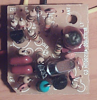
Sometimes you need to get the schematic from a manufactured PCB. It is always a pain in the neck, but I will show a method that could help you.

It is basically to get a netlist. Of course this method is valid for only one or two layers PCB. In case you have a four layer PCB it is a bit tough to get it.

Let's start with a simple one layer board because it is easy to explain:


Fig.1: Simple one-layer PCB from a toy car transmitter
Picture from electronicayciencia.blogspot.com.es
   
1. The first step is assigning a number to each PCB track


Fig. 2: Assign a number to each track
Picture from electronicayciencia.blogspot.com.es

2. Second step is numbering the components and connectors. Many of the components could be already labeled as C1, R3 or D2. You should also assign a name to each connector.

3. Third step is to build a matrix table (aka netlist) where rows are components and colums are the previously numbered PCB tracks. 
You can mark resistor pins as X, diode pins as A and K, transitor pins as E, B, C, and so on. 
It is also a good idea to highlight both VCC and GND tracks. 


Fig. 3: Netlist or matrix connections table. It is a good idea to indicate the number of pins of each component and then count all of them to check there are no missing connections in your netlist
Picture from electronicayciencia.blogspot.com.es

4. Fourth step is now drawing the netlist on your schematic design program. You can place all the components, create the VCC and GND nets and then connect the components to the net symbols.

For those tracks with only two connections, you can place a wire directly. 
For the tracks with three or more connections, you can use net names.
I recommend you to use the same net names as the track numbers. 

5. Next step is try to recognize the circuit, so you can place the components better. This step depends on your experience. 
In this case, there is an astable oscillator, so we place the components in its usual form. 
It is very important to place the components in such way you can easily recognize their function. Otherwise you will only have a mess of wires. 


Fig. 4: Schematic done from the netlist. Try to represent or group the circuit in such way you can identify some functions.
Picture from electronicayciencia.blogspot.com.es

6. Finally you should export your netlist from the schematic and then compare it with your initial netlist. Both tables should match. Otherwise you did something wrong. 

Depending on your schematic design program (Altium, Eagle, kicad, orcad, etc) you will get a different netlist format, but most of them are in the same way:

rR1 5  0     100
rR2 11 0     1200
qQ1 4  6  5  2SC945
dD1 0  VSS   1N4148

First item is the component name. Then are the net connections (in this case 0 is GND) and the last column is the value or reference.  


Sunday, June 8, 2014

Component Signature Analyzer

I'll start this blog with a post about my current project: a component signature analyzer

Many of you maybe already know about it, but the signature analysis (also known as V-I testing) it's really useful when repairing electronic devices. 

The main advantage when testing a board with a V-I tester is that the device under test (usually called DUT) doesn't need to be powered up. So this technique is great for evaluating non-working boards.

What I will basically do is a resistor selector board that allows to change the current over the DUT. Then, modifying the frequency you can display a good signature on the oscilloscope display.

So basically what you'll need is a sine wave generator (from 10Hz to 50Hz), an oscilloscope with X/Y mode and a simple resistor.


Fig. 1: For displaying analog signatures, a variable-frequency and voltage signal source, a resistor and an oscilloscope with X/Y mode are required. The voltage drop across the device under test (DUT) drives the display in the X axis, while the measured current through the DUT drives the display's Y axis.
Picture from electronicproducts.com

So then each component will produce a different signature, depending on the current flow and the applied voltage. There are four basic Component Analog Signatures: resistance, capacitance, inductance, and semiconductance (Fig. 2). Recognizing these four basic unique signatures on the oscilloscope display is one of the keys to successful dead-boards troubleshooting.


Fig. 2:The analog signatures shown here for resistance (a), capacitance (b), inductance (c), and semiconductance (d) show typical shapes. Actual shapes may vary, but having an analog signature for a device onknown-good board lets users compare the shape of the DUT's analog signature to see if there is a deviation indicative of a fault.
Picture from electronicproducts.com


Of course there are excellent devices such as the Huntron Tracker which already integrate the function generator and the oscilloscope display in only one device, but they are really expensive (more the $7000 USD). So with a cheap function generator such as the Victor VC 2002 (127,19€) and a secod-hand Tektronix TDS210 (437,18€) I'll try to do exactly the same as the Huntron does. 

Next post will be my schematic, the PCB and some info about my Component Signature Analyzer. Meanwhile I leave here some useful links: