It is basically to get a netlist. Of course this method is valid for only one or two layers PCB. In case you have a four layer PCB it is a bit tough to get it.
Let's start with a simple one layer board because it is easy to explain:
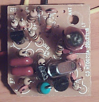
Fig.1: Simple one-layer PCB from a toy car transmitter
Picture from electronicayciencia.blogspot.com.es
1. The first step is assigning a number to each PCB track

Fig. 2: Assign a number to each track
Picture from electronicayciencia.blogspot.com.es
2. Second step is numbering the components and connectors. Many of the components could be already labeled as C1, R3 or D2. You should also assign a name to each connector.
3. Third step is to build a matrix table (aka netlist) where rows are components and colums are the previously numbered PCB tracks.
You can mark resistor pins as X, diode pins as A and K, transitor pins as E, B, C, and so on.
It is also a good idea to highlight both VCC and GND tracks.

Fig. 3: Netlist or matrix connections table. It is a good idea to indicate the number of pins of each component and then count all of them to check there are no missing connections in your netlist
Picture from electronicayciencia.blogspot.com.es
4. Fourth step is now drawing the netlist on your schematic design program. You can place all the components, create the VCC and GND nets and then connect the components to the net symbols.
For those tracks with only two connections, you can place a wire directly.
For the tracks with three or more connections, you can use net names.
I recommend you to use the same net names as the track numbers.
5. Next step is try to recognize the circuit, so you can place the components better. This step depends on your experience.
In this case, there is an astable oscillator, so we place the components in its usual form.
It is very important to place the components in such way you can easily recognize their function. Otherwise you will only have a mess of wires.

Fig. 4: Schematic done from the netlist. Try to represent or group the circuit in such way you can identify some functions.
Picture from electronicayciencia.blogspot.com.es
6. Finally you should export your netlist from the schematic and then compare it with your initial netlist. Both tables should match. Otherwise you did something wrong.
Depending on your schematic design program (Altium, Eagle, kicad, orcad, etc) you will get a different netlist format, but most of them are in the same way:
rR1 5 0 100
rR2 11 0 1200
qQ1 4 6 5 2SC945
dD1 0 VSS 1N4148
First item is the component name. Then are the net connections (in this case 0 is GND) and the last column is the value or reference.
No comments:
Post a Comment